MCP4922 Dual 12-Bit, Buffered DAC
The MCP4922 is a 12-bit, high accuracy, low noise performance, buffered voltage output Digital-to-Analog Converter (DAC). This is an SPI-compatible Serial Peripheral Interface device with a 2.7V to 5.5V supply. The MCP4922 comes with a shutdown pin, The user can shut down both DAC channels by using this pin or shut down the DAC channel individually. This helps to reduce the power consumption of DAC circuits. We can configure the full-scale range by setting the Gain Selection Option bit, and it includes double-buffered registers for synchronous updates of two DAC outputs using the LDAC pin. The MCP4922 comes with a Power-on Reset (POR) circuit to ensure reliable powerup. The IC is based on resistive string architecture which helps to achieve low differential non-linearity (DNL) error and fast settling time, which is very useful in precision applications. This device can be operated up to 125°C. The MCP4922 is available in the PDIP, SOIC and TSSOP packages.
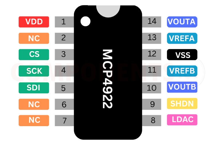
MCP4922 Pinout Configuration
Here are the pinout details for MCP4922.
| Pin Number | Name | Function |
| 1 | VDD | Supply Voltage Input (2.7V to 5.5V) |
| 2 | NC | No Connection |
| 3 | CS | Chip Select Input |
| 4 | SCK | Serial Clock Input |
| 5 | SDI | Serial Data Input |
| 6 | NC | No Connection |
| 7 | NC | No Connection |
| 8 | LDAC | Synchronization Input |
| 9 | SHDN | Hardware Shutdown Input |
| 10 | VOUTB | DACB Output |
| 11 | VREFB | DACB Reference Voltage Input (VSS to VDD) |
| 12 | VSS | Ground reference point for all circuitry on the device. |
| 13 | VREFA | DACA Reference Voltage Input (VSS to VDD) |
| 14 | VOUTA | DACA Output |
Features of MCP4922
MCP4922 DAC chip has the following key features:
- Rail-to-Rail Output
- SPI Interface with 20 MHz Clock Support
- Simultaneous Latching of the Dual DACs with LDAC pin
- Fast Settling Time of 4.5 µs
- Selectable Unity or 2x Gain Output
- External Voltage Reference Inputs
- External Multiplier Mode
- 2.7V to 5.5V Single-Supply Operation
- Extended Temperature Range: -40°C to +125°C
Manufacturers of MCP4922:
The MCP4922 is manufactured Microchip Technology.
MCP4922 Equivalents
If you are looking for an equivalent replacement for MCP4922, you could check out the MCP4902 and MCP4912 from the same family.
MCP4922 Alternatives
If you are looking for an alternative for MCP4922 you can look at the other IC from these.
MAX5216, DAC8562, MCP4725, MCP4921, PT8211, DAC0832, DAC0808, DAC7715, AD5737, AD5421.
Note: Complete technical details can be found in the MCP4922 datasheet at this page’s end.
MCP4922 Circuit Diagram
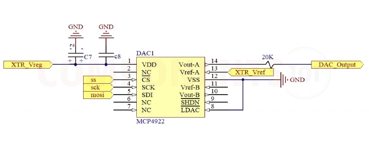
Here is a simple circuit diagram for the MCP4922 DAC. In the we are only using one output. But you can follow the same scheme for the other channel too. Two bypass capacitors are added to the power supply in order to filter high-frequency noise. The SPI pins are connected to the MCU. An external reference voltage is provided to the Vref pin. For the MCP4922 Arduino interfacing you can use the MCP4922 Arduino Library.
MCP4922 Troubleshooting Guide
My MCP4922 is not providing any output. What could be the issue?
First, ensure that the power supply voltages are within the specified range (2.7V to 5.5V). Check the connections to the MCP4922, including vss, vdd, and the reference voltages. Set the output to the desired value over SPI.
MCP4922 circuit performance is not stable. What might be causing this?
This could be caused by several factors. Here are some possible causes to consider,
- Ensure that the power supply to the MCP4922 is stable and within the specified range. Fluctuations in the power supply voltage can lead to instability.
- Proper grounding is essential for the stability of the MCP4922. Ensure that the ground connections are solid and that there are no ground loops.
- If you're using SPI to communicate with the MCP4922, ensure that the communication is reliable. Check the SPI connections and verify that the correct data is being sent to the MCP4922.
How to reduce the noise while using MCP4922?
- Place capacitors (typically 0.1 µF) close to the power supply pins (VDD and VSS) of the MCP4922 to filter out high-frequency noise.
- Use a low-noise power supply for the MCP4922 and other sensitive components in your circuit.
- Ensure proper grounding practices, such as using a solid ground plane and minimizing ground loops, to reduce noise.
- Connect unused inputs of the MCP4922 to the ground (for the DAC A/B inputs) or to VREF (for the DAC B input) to prevent noise pickup.
Things to Consider When Using MCP4922 in your Design:
When designing with the DAC8562, a 16-bit Analog-to-Digital Converter (ADC), here are some important considerations and design tips to keep in mind:
Layout Guidelines
Inductively coupled AC transients and digital switching noises can degrade the input and output signal integrity, and potentially reduce the device performance. A careful board layout will minimize these effects and increase the signal-to-noise ratio (SNR). Bench testing has shown that a multi-layer board utilizing a low-inductance ground plane, isolated inputs and isolated outputs with proper decoupling, is critical for the best performance. Particularly harsh environments may require shielding of critical signals. Breadboards and wire-wrapped boards are not recommended if low noise is desired.
Power Supply Recommendations
The typical application will require a bypass capacitor in order to filter high-frequency noise. The noise can be induced onto the power supply’s traces from various events such as digital switching or as a result of changes in the DAC’s output. The bypass capacitor helps to minimize the effect of these noise sources. The above figure illustrates an appropriate bypass strategy. In this example, two bypass capacitors are used in parallel: (a) 0.1 µF (ceramic) and (b) 10 µF (tantalum). These capacitors should be placed as close to the device power pin (VDD) as possible (within 4 mm). The power source supplying these devices should be as clean as possible. If the application circuit has separate digital and analog power supplies, VDD and VSS should reside on the analog plane.
Applications of DAC MCP4922
- Set Point or Offset Trimming
- Precision Selectable Voltage Reference
- Motor Control Feedback Loop
- Digitally Controlled Multiplier/Divider
- Calibration of Optical Communication Devices
MCP4922 Ordering Information
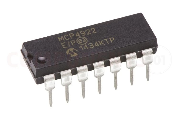
MCP4922-E/P indicates the DIP package while MCP4922-E/SL indicates the SOIC package, and the MCP4902-E/ST indicates the TSSOP package. You might also come across MCP4922T-E/SL and MCP4902T-E/ST, they are the same as above, the only difference is that they come in Tape and Reel.
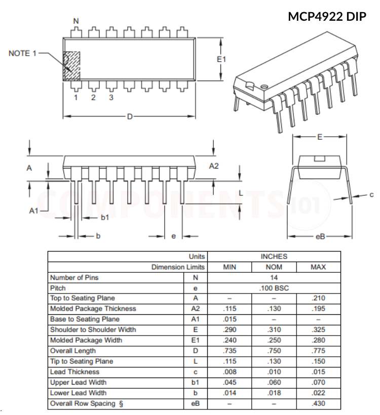
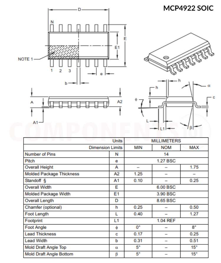
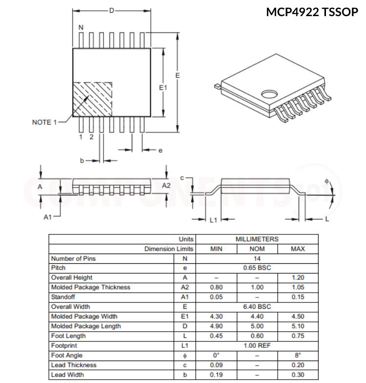
MCP4922 Footprint and Package Information
Here you can find the mechanical drawings of MCP4922 along with its dimensions. The dimensions can be used to create custom footprints of the module and be used for PCB or CAD modelling.